Former Projects
EU Project: VERy high Throughput Satellite-Ground Optical Link (VERTIGO)
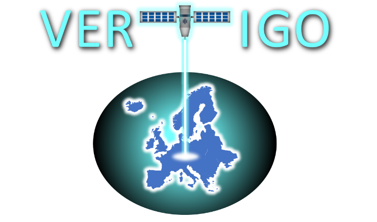
VERTIGO is a 3-years H2020 collaborative project that aims to develop and demonstrate concepts allowing for a significant capacity increase of satellite feeder links through the use of state-of-the-art optical technologies. VERTIGO will address the key enabling technologies (high optical power generation, high efficiency waveforms, atmospheric impairments mitigation) for the implementation of high throughput optical links and test them in ground indoor and outdoor demonstrations thanks to a fully complementary consortium. Partners include Creonic GmbH (Germany), ETH Zürich (Switzerland), Fraunhofer HHI (Germany), Gooch and Housego Ltd, LEO Space Photonics R&D (Great Britain), ONERA (France), Thales Alenia Space in France and Switzerland and Thales Research & Technology. Next generation satellite systems will play a key role to bridge the digital divide and offer high speed connectivity for all by 2025. In this context, optical feeder links are considered as a very promising technology to meet the future VHTS system requirements. VERTIGO ambitions to pave the way towards very high throughput satellite systems and contribute to maintain EU technological leading edge and industry competitiveness.
external page Project Website
Technical manager: Prof. Dr. Juerg Leuthold, ETH Zurich
Project manager: Dr. Benedikt Bäuerle, Dr. Maurizio Burla, ETH Zurich
Coordinator: Thales Alenia Space France SAS, France
Project number: 822030, H2020-SPACE-2018
Topic: SPACE-15-TEC-2018 - Satellite communication technologies
Timeframe: 06/2020 – 11/2022
InnoSuisse Project: Ion Beam Sputtering of 2D Materials – A New Approach
The InnoSuisse project “Ion Beam Sputtering of 2D Materials – A New Approach” tackles the direct growth of different 2D materials by means of Ion Beam Sputtering.
Since the emergence of graphene in 2004, a whole new research field into 2D materials has opened up. The potential applications for 2D materials include mechanical reinforcements, the use as additives to chemical modifiers and future electronics and opto-electronics. The expected future impact of 2D materials is immense across all scientific and industrial fields.
Successful implementation of 2D materials requires coating technologies which enable the large scale, on-demand synthesis of high quality crystalline monolayers on a substrates of choice. No presently applied coating technology fulfills all these requirements at the same time. The aim of this project is to develop a new approach to deposit 2D materials based on a physical vapour deposition technique, namely ion beam sputtering (IBS). A novel, tailor-made research coating tool will be designed, commissioned and tested for direct growth of 2D materials on different substrates.
Technical manager: Prof. Dr. Juerg Leuthold, ETH Zurich
Project manager: Stefan Köpfli, ETH Zurich
Coordinator: Dr. Thomas Gischkat, RhySearch
Project number: 47744.1 IP-ENG
Topic: Advanced Manufacturing
Timeframe: 10/2020 – 03/2022
EU Project: Wafer-scale, CMOS integration of photonics, plasmonics and electronics for mass manufacturing 200Gb/s NRZ transceivers towards low-cost Terabit connectivity in Data Centers (plaCMOS)
The goal of the plaCMOS project is to develop a powerful integration technology integrating novel modulators, photodetectors and related electronics in a super-fast, micrometer-scale optical engine capable of transmitting and receiving NRZ data at world’s fastest speed of 200 Gbit/s per optical channel. plaCMOS will rely on this breakthrough advancement, to demonstrate scalability of thermally independent multi-transceiver chips paving the way for next generation Tbit/s transceivers in monolithic chips complying with industry standards while surpassing performance expectations.
plaCMOS’s technology speed and scalability advantages will be validated in fully functional single- channel and multi-channel (CWDM-based and in SDM-based) transceiver prototype assemblies, clearly addressing both technology roadmaps for future data centers, waiving the stringent requirements for high-port count front panels in switches and servers at the best cost/performance intersection. In the same context, plaCMOS will explore the application of its PIC platform in forward looking applications that can lead to more advanced reconfigurable transceivers.
Technical manager: Prof. Dr. Juerg Leuthold, ETH Zurich
Project manager: Dr. Ping Ma, ETH Zurich
Coordinator: Dr. Elad Mentovich, Mellanox Technologies, Ltd.
Project number: 980997, H2020-ICT-2017-1
Topic: ICT 30-2017 Photonics KET (PIC)
Timeframe: 12/2017 - 02/2022
COST Action: European Network for High Performance Integrated Microwave Photonics
Next generation global telecommunication platforms and emerging massive take-up applications in radar, communications and space industries will require entirely new technologies to address the current limitations of electronics for massive capacity and connectivity. Multigigabit-per-second 5G wireless communications, the Internet of Things, the upcoming Smart Car scenarios and satellite payloads will require a full convergence between optical fibre and wireless segments.
Microwave photonics (MWP) combines RF and photonics and is the best positioned technology to carry out this convergence. Current MWP systems, however, are fiber and discrete-component based, which limits energy-efficiency, flexibility and scalability, and, as a result, high volume application. Integrated Microwave Photonics (IMWP) seeks to address these limitations by incorporating these systems into photonic integrated circuits (PICs). IMWP is still at its infancy and a considerable body of knowledge, technical and scientific roadmaping and interactions between industry academia need to be developed during the next years.
The European Network for High Performance Integrated Microwave Photonics (EUIMWP) Action aims to shape and bring the relevant IMWP community supporting coordination and networking actions to consolidate this new IMWP ecosystem, providing exchange of knowledge, ideas and delivering a portfolio of technological benchmarkings to establish performance indicators defining future technological requirements in high performance scenarios such as 5G, automotive and aerospace technologies.
The action brings together groups from academia, industry and transnational organizations with complementary competences and on a global scale including PIC and MWP experts, microwave system application designers and end-users to fully develop the synergies required by this new paradigm. external page Project Website
Chair of the action: Prof. Dr. José Capmany, ITEAM Research Institute, Spain
Short Term Scientific Mission Coordinator: Dr. Maurizio Burla, ETH Zurich
Project number: CA16220
Timeframe: 10/2017 - 10/2021
SNSF Ambizione Project: Millimeter-Wave On-Chip Wireless-Optical Transceivers for 5G Wireless Communications
The goal of this project is to create the first integrated microwave photonics (MWP) transceivers, operating at mm-wave frequencies, with direct optical-to-wireless and wireless-to-optical conversion and beam steering capability. This project targets the creation of a novel enabling technology for high capacity millimeter-wave and THz wireless communications, through integration of electronics, photonics and antennas, opening the path towards ultra-broadband transceivers at a low unit cost and deployable at large scale.
Project Leader: Dr. Maurizio Burla, ETH Zürich
Project number: 173996
Timeframe: 1/10/2017 - 1/9/2021
ERC project: Plasmonic -Silicon-Organic Hybrid - a Universal Platform for THz Communications (PLASILOR)
The PLASILOR project brings together the fields of silicon photonics, organic materials and plasmonics. The aim is the development of a novel plasmonic silicon-organic-hybrid platform that meets the performance expectations for next generation devices, leveraging at once the large-scale integration and low-cost characteristics of silicon, the processing functionalities offered by organic materials and the ultra-compact size and ultra-high speed of plasmonic devices. The outcome will enable the creation of disruptive technologies for next-generation THz communications and applications, including biosensing, imaging, spectroscopy, high-speed chip-to-chip communications, and more. See also the project website.
Coordinator: Prof. Dr. Juerg Leuthold, ETH Zürich
Project manager: Dr. Maurizio Burla, ETH Zürich
Project number: 670478
Timeframe: 11/2015 - 10/2020
EU Project: Microwave Microscopy for Advanced and Efficient Materials Analysis and Production (MMAMA)
Work Package 3: Nanoscale and Microscale Modelling – Bridging the Gap
The main goal of this project is to enable modeling and simulation of semiconductor structures within a large “classical” 2-D and 3-D electromagnetic models at the microwave and optical frequencies. The modeling and simulation aims at structures involving a planar semiconductor structures, a sharp metallic tip with a radius of 5-100nm, and a millimeter long wire with a diameter of 0.5mm.
In the frame of this project an efficient and accurate numerical field solver for coupling Maxwell equations with semiconductor equations in time domain should be developed. The development is based on the existing self-developed time domain vector DG-FEM solver available at the IEF.
external page Project Website
Project manager: Dr. Jasmin Smajic, ETH Zürich
Coordinator: Prof. Dr. Kamel Haddadi, University of Lille
Project number: 761036, H2020-NMBP-2017
Topic: NMBP-07-2017 - Systems of materials characterisation for model, product and process optimisation
Timeframe: 11/2017 - 10/2020
SNF Project: Design and Manufacturing of Heterogeneous Photonic Composites for Aerospace Applications

Photonic crystal structures (PCS) allow control of the response to electromagnetic irradiation by the structural design. A proper design enables many important applications. So, high-temperature stable PCS have a high potential as heat protection coatings for space vehicles during atmospheric reentry, and also offer useful coatings for gas turbine blades or selective emitters for thermophotovoltaics. Thermal protection systems (TPS) in space vehicles are of relevance because electromagnetic radiation from ionized gas in the shock layer at reentry to the Earth atmosphere can constitute up to 30-50% of the overall heat flux, albeit for relatively short times. For Jupiter entries, almost the entire heating is due to electromagnetic radiation. Ideally, the design of PCS for TPS should be tuned to the radiation spectra for the frequencies that are specific to the specific reentry conditions.
In the previous work along the ETH-NASA Agreement, several photonic TPS (pTPS) types were theoretically studied at the Institute of Electromagnetic Fields (IEF) of ETH. All of them were optimized for the spectral range comprising the highest power part of the shock gas irradiation. As candidates for pTPS, multilayer stacks, inverse opals, woodpiles, porous reflectors, and guided-mode resonance (GMR) structures were identified. In this project, the suggested pTPS will be further refined at the IEF and ultimately fabricated at the Laboratory of Complex Materials (CM) at ETH. The fabrication of pTPS is the core of this project. Optical properties of the selected pTPS materials will be tailored to reflect a broader part of the hot gas spectrum, including the VUV/UV part.
Coordinator: Dr. Valery Shklover, ETH Zurich
Project Leader: Prof. Dr. Juerg Leuthold, ETH Zurich
SNF project Nr: 200021_160184
Timeframe: 09/2015 - 09/2020
CTI project: Optical Sensor
The scope of this project is to develop a miniature optical sensor. We apply photonic technologies pioneered at our institute to create next-generation sensing concepts. Our goal is to use photonics to develop radically integrated sensing concepts, which can be used in a variety of contexts, e.g. in biological and chemical environments.
Coordinator: Prof. Dr. Juerg Leuthold, ETH Zurich
Project Manager: Alexander Lochbaum, ETH Zurich
Project number: 19067.1
Timeframe: 10/2016 - 10/2019
ETH Fellowship: Novel Highly Scalable Optical Interconnect Solution
An ultra-dense high-capacity fiber link for optical interconnect transmissions will be demonstrated by combining three multiplexing transmission schemes, i.e. wavelength division multiplexing, space division multiplexing and mode division multiplexing. Since each multiplexing technique is independent and can be implemented simultaneously, the transmission capacity scales very favorably by the multiplication of channel numbers for each multiplexing scheme. This scaling by the power x3 is additionally complemented by implementing the interconnect technology in a novel miniaturized plasmonic integration platform.
Host: Prof. Dr. Juerg Leuthold, ETH Zurich
Project Manager: Dr. Tatsuhiko Watanabe, ETH Zurich
Project number: 16-2 FEL-51
Timeframe: 04/2017 - 03/2019
ETH project: Atomic Scale Photonic Switch
The project suggests the development of a new gate controlled atomic scale plasmonic-switch platform. The proposal builds on a recent experiment by the authors, where they found an impressive digital switching when electrically relocating a single (or at least few) atom(s) in a plasmonic wire waveguide. Initial experiments have shown a reproducible and reliable operation for days. The structure is CMOS compatible and is derived from a standard memrestive structure such as known for electronics. The discovery allows for the first time to scale down optical switches with an extraordinary performance to dimensions way below 1 µm2 – and thus bringing photonics much closer to the electronic scale. This project proposes to continue an existing research effort, which has the potential to initiate a paradigm-shift in photonics: the suggested structures are orders of magnitude smaller than what is known in optics with a power consumption at the fJ level for a single switch operation.
Coordinator: Prof. Dr. Juerg Leuthold, ETH Zurich
Project Manager: Dr. Alexandros Emboras, ETH Zurich
Project number: ETH-35 15-2
Timeframe: 04/2016 - 03/2019
EU project: PLASMOfab, a generic CMOS-compatible platform for co-integrated plasmonics/photonics/electronics PICs towards volume manufacturing of low energy, small size and high performance photonic devices.

PLASMOfab aims to address the ever increasing needs for low energy, small size, high complexity and high performance mass manufactured PICs by developing a revolutionary yet CMOS-compatible fabrication platform for seamless co-integration of active plasmonics with photonic and supporting electronic. The CMOS-compatible metals Aluminum, Titanium Nitride and Copper, will be thoroughly investigated towards establishing a pool of meaningful elementary plasmonic waveguides on co-planar photonic (Si, SiO2 and SiN) platforms along with the associated photonicplasmonic interfaces. The functional advantages of PLASMOfab technology will be practically demonstrated by developing two novel functional prototypes with outstanding performances: 1) a compact, plasmonic bio-sensor for label-free inflammation markers detection with multichannel capabilities and record-high sensitivity by combining plasmonic sensors with electrical contacts, Si3N4 photonics, high-speed biofunctionalization techniques and microfluidics 2) a 100 Gb/s NRZ transmitter for datacom applications by consolidating low energy and low footprint plasmonic modulator and ultra high-speed SiGe driving electronics in a single monolithic chip. The new integration technology will be verified through waferscale fabrication of the prototypes at commercial CMOS fabs, demonstrating volume manufacturing and cost reduction capabilities. PLASMOfab technology will be supported by an EDA software design kit library paving the way for a standardized, fabless plasmonic/photonic IC eco-system.
Project manager: Ueli Koch, ETH Zurich
Coordinator: Prof. Dr. Nikos Pleros, Aristotle University of Thessaloniki
Project number: 688166, H2020-ICT 2015
Topic: ICT-27-2015 - Photonics KET
Timeframe: 1/2016 - 12/2018
Industry Solutions: Group specializing in industry-oriented scientific projects
The topics of interest of our group are new functional materials for industrial applications. Our expertise includes Thermal barrier coatings, Protection coatings for atmospheric reentry, High-temperature materials, Photonics, High-temperature photonics, Superhard coatings, Materials with anisotropic heat dissipation, Energy conversion and storage, Nanostructures and Nanofluids, Reactivity in solids, Organic/Inorganic materials, Molecular electronics. This expertise is confirmed by more than 300 publications in pierreviewed journals, about 20 reviews and 12 patents. We perform conceptualization, characterization and chemical and solid-state synthesis of new functional materials for industrial applications. The characterization methods we apply comprise single crystal and powder crystallography, in situ X-ray measurements at high temperature and under controlled atmosphere, high-resolution scanning and transmission electron microscopy, dilatometry, DTA, measurement of physical properties of crystals, powders and films. Modeling includes study of heat transport and heat dissipation, spectroscopy, phase analysis, electromagnetic, band structure and force-field calculations. The group is working very close to industries.
More information
Group lead: Dr. Valery Shklover
Timeframe: 1/2000 - 12/2018
SNF project: Plasmonic Active Devices based on Metal Oxides (PADOMO)

The PADOMO project aims to develop innovative active photonic devices by properly integrating high quality materials providing large nonlinear effects. It is expected that the outcome of the project achieves significant technological advancements against state-of-the-art nonlinear device designs, with respect to the energy consumption, device speed, thermal stability, device size, and current technology compatibility. The project holds the promise to pave the way to a high-impact real-world-driven technology for active photonic devices.
Coordinator: Prof. Dr. Juerg Leuthold, ETH Zürich
Project Manager: Dr. Ping Ma, ETH Zürich
Project Number: IZCJZ0-158197
Timeframe: 09/2015 - 08/2018
ETH project: Mid-Infrared Quantum Emitter - Ultra-compact, Low-cost, and CMOS-Compatible Sources in the Mid-Infrared
In this project, we explore novel approaches for the realization of CMOS-compatible quantum emitters in the mid-infrared (mid-IR) spectral window. The mid-IR spectral window from 3 μm to 5 μm is of fundamental interest for various applications in the fields of environmental sensing, health sciences, material sciences and physics. The project aims to make mid-IR applications accessible to the CMOS industry. This would have a considerable impact on many industries, where so far high-end solutions for mid-IR emitters, e.g. those based on quantum cascade lasers, are not commercially viable for large-scale applications. The quest for a compact and CMOS-compatible mid-IR source is addressed by considering multiple new and promising approaches. The strength of two institutes at ETH, the Institute for Integrated Systems (Prof. Wood) bringing an expertise in colloidal quantum dots (CQDs), and the Institute of Electromagnetic Fields (Prof. Leuthold), bringing an expertise in CMOS photonics devices fabrication, are combined to build novel light emitter in the mid-IR.
Coordinator: Prof. Dr. Juerg Leuthold, ETH Zurich
Project Manager: Alexander Lochbaum, ETH Zurich
Project number: ETH-45 14-2
Timeframe: 03/2015 - 08/2018
SNF project: On-chip coherent light sources based on nonlinear frequency conversion in thin organic two-dimensional crystals (precoR)
This project aims at the on-chip generation of signals by means of nonlinear frequency conversion employing novel thin nonlinear polymer/monomer materials incorporated into strong-confinement low-loss plasmonic waveguide structures. The new ultra-compact coherent light source holds promise to cover a broad range of frequencies spanning from the ultra-violet to the far infrared and will allow to access spectral regions which are not attainable with the currently available conventional lasers.
Coordinator: Prof. Dr. A. Dieter Schlüter, Institute of Polymers, ETH Zürich
Timeframe: 08/2014 - 08/2017
EU-Japan project: Functional Thin-Film Ferroelectric Materials for CMOS Compatible Photonics (FF-Photon)

The FF-Photon project investigates the light-matter interaction of epi-grown thin-film ferroelectric materials and develops the related manufacturing and characterization technologies. As an outcome of the project we envision a deep and comprehensive understanding of the photo-responsive process of ferroelectric thin-films and the establishment of a platform for CMOS compatible ferroelectric thin-films and enabled innovative optical devices.
Coordinator: Prof. Dr. Juerg Leuthold, ETH Zürich
Project Manager: Dr. Ping Ma, ETH Zürich
Project Number: 200021_159565
Timeframe: 10/2014 - 03/2017
Various fundings: Open source software for computational electromagnetics
The Open Source package OpenMaXwell is a graphic platform for computational electromagnetics including 2D and 3D FDTD solvers, static FD solvers, and the most advanced 2D and 3D MMP solvers. It can handle various applications, including eigenvalue problems (resonators, cylindrical and periodic waveguide structures, photonic crystals), scattering, plasmonics, antennas, etc.
Principle Investigator: Prof. Dr. Christian Hafner, ETH Zürich
Timeframe: 2009 - 2017
Euramet-Project IND51: Metrology for optical and RF communication systems (MORSE)

Traffic on telecommunication networks is currently growing by around 40 % each year, which will soon lead to a capacity crunch unless new technologies are introduced to maintain quality and prevent disruption to the networks on which the modern world relies. Technologies such as reconfigurable and multiple antennas can increase the capacity and quality of wireless communications, however they also make testing more complex and time consuming. When building a satellite, antenna testing happens during a high-risk stage of development, therefore more complicated antennas could potentially disrupt the already tight delivery schedules satellite companies must adhere to. This project will support the work of the European Telecommunications Standards Institute (ETSI) and the International Electrotechnical Commission (IEC), and will result in new measurement procedures and services to support the introduction of new multiple antenna systems, satellite system testing and the next generation of optical communications equipment.
external page More information
Coordinator: David Humphreys (NPL)
Timeframe: 2013 - 2016
EU-Project: Flexible Optical Cross-connect Nodes enabling next generation flexible optical networking (FOX-C)
The FOX-C project aims to design, develop and evaluate the first functional system prototype of flexible add-drop multiplexers and flexible optical cross-connectsThe FOX-C project aims to design, develop and evaluate the first functional system prototype of flexible add-drop multiplexers and flexible optical cross-connects with fine switching granularity at the optical subcarrier level with the purpose to enable the end-to-end network routing of any tributary channel with flexible bandwidth down to 10Gb/s carried over wavelength superchannels, each with an aggregated capacity beyond 1Tb/s. Moreover, the project will define and evaluate the flexible transmission solutions and their exact characteristics, thus providing a holistic flexible optical networking approach applicable in next generation networks.
external page More information
Coordinator: George Papastergiou
Project Manager: Benedikt Baeuerle, Arne Josten, ETH Zurich
Timeframe: 10/2012 - 12/2015
ETH CHIRP Project: Computational nano-optics - Shape calculus and inverse problems
This project aims to devise and extend numerical methods for important applications in nano-optics, namely plasmonic structures such as nano antennas, scanning near-field optical microscopy (SNOM), etc. It employs the most advanced techniques of computational mathematics namely hp-FEM computations, shape gradients, Dirichlet to Neuman maps, matrix compression, etc.
Principle Investigator: Prof. Dr. Ralph Hiptmair, SAM, ETH Zürich
Timeframe: 2012 - 2015
SNF project: Light-trapping enhanced solar cells for outer planets missions
In this project, we design and study solar cells that might be useful for missions to outer planets, where the light intensity is small and temperature is low. We expect that also terrestrial photovoltaics will benefit from these findings. Especially different spectrum-splitting schemes seem to be promising and are optimized by extensive simulations combined with numerical optimizers.
Principle Investigator: Prof. Dr. Christian Hafner, ETH Zürich
Timeframe: 2012 - 2015
EWZ project: Metamaterials and coupled resonator systems
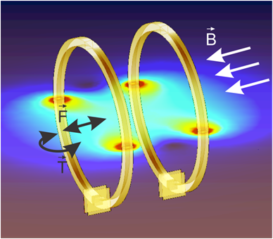
Systems of coupled electromagnetic resonators lead to various interesting effects. When arranging the resonators on some lattice, photonic crystals and more general artificial materials or metamaterials are obtained. We study the electromagnetic properties of these systems and optimize them for applications such as shielding of electrosmog, absorption, filtering for spectrum splitting, etc. We also study the forces between coupled resonators and have employed them for creating wireless motors.
Principle Investigators: Prof. Dr. Juerg Leuthold, ETH Zürich
Prof. Dr. Christian Hafner, ETH Zürich
Timeframe: 2006 - 2015
EU-Project: Nano Scale Disruptive Silicon-Plasmonic Platform for Chip-to-Chip Interconnection (NAVOLCHI)
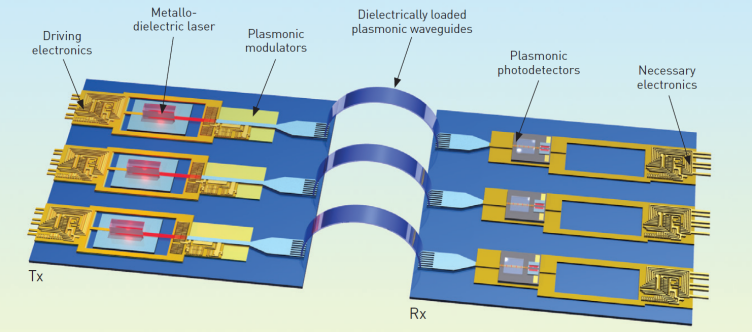
NAVOLCHI explores a novel nano-scale plasmonic chip-to-chip and system-in-package interconnection platform to overcome the bandwidth, foot-print and power consumption limitations of today's electrical and optical interconnect solutions. NAVOLCHI will be a significant resource of know-how on the plasmonic modulators domain and relating materials.
Project Manager: Claudia Hoessbacher, ETH Zurich
Coordinator: Prof. Dr. Manfred Kohl, Karlsruhe Institute of Technology
Former Coordinator: Prof. Dr. Juerg Leuthold, ETH Zurich
Timeframe: 11/2011 - 10/2014
EU-Project: Embedded Resonant and Modulable Self-Tuning Laser Cavity for Next Generation Access Network Transmitter (ERMES)

For the next generation access network wavelength division multiplexed passive optical networks (WDM-PON) appear a promising solution offering almost unlimited bandwidth similarly to point-to-point links, while allowing the advantages of fiber sharing. WDM-PON deployment requires colourless optical network unit (ONU) transmitters, so that each user has the same transmitter. Up to now, these characteristics have been unsatisfactorily obtained either with a costly tunable transmitter or by exploiting external seeding sources. ERMES proposes a disruptive approach to the ONU transmitter. The breakthrough idea is to use a significant portion of the network to implement an embedded self-tuning modulable laser cavity.
Coordinator: Mario Martinelli, Politecnico di Milano
Timeframe: 9/2011 - 8/2014